Applications
ENABLING NEXT-GENERATION SEMICONDUCTORS AND DEVICES
Market demand for faster, smaller, more powerful, and energy-efficient electronics is driving the development of new approaches to product manufacturing which are packed with advanced features and new capabilities. Creating these new cutting-edge devices and other technologies is extremely challenging and requires the adoption of new approaches.
DJ MicroLaminates continues to enable the development of these new devices with new capabilities along with new requirements from manufacturers. Our innovative thin and thick dry film resist sheets have fostered the delivery of a wide range of applications – from advanced MEMS, medical and microfuidics, electronics and passive devices, and wafer level packaging.


SEMICONDUCTORS & INTERCONNECT
As devices get smaller and components (transistors, capacitors, etc.) on a chip get packed closer together, the only way to build is vertically. In order to produce state-of-the-art, high-performance electronic devices, structures with narrow geometries and multiple, complex layers are now designed and need to be manufactured. These require increasingly flexible, lower cost, greener and more economical processes. An approach that uses thin or thick dry film sheets can increase both component density and productivity, and address other requirements as needed.
PATTERNING & PACKAGING
Both patterning (including especially photolithography but also deposition and etch) and packaging (forming a protective enclosure around a finished chip and also creating the external connections for input/output) involves a set of process steps that produce extremely small, intricate, high aspect ratio features in integrated circuits. As device dimensions continue to shrink, advanced structures will require advanced lithography and wafer-level packaging facilitated by thin and especially, thick films.
CONSUMER ELECTRONICS
Consumer or home electronics are everyday devices used for entertainment, communications and recreation. Audio devices, calculators, digital cameras, watches, displays, headphones and VR headsets, tablets, smartphones, televisions and many similar products and accessories are in widespread use today. Growing consumer demand for lighter, faster devices with excellent viewing and listening options and increased capabilities drives manufacturers to innovate by building more jam-packed advanced structures on their devices, requiring advanced lithography based on thin and thick film.
MEDICAL DEVICES
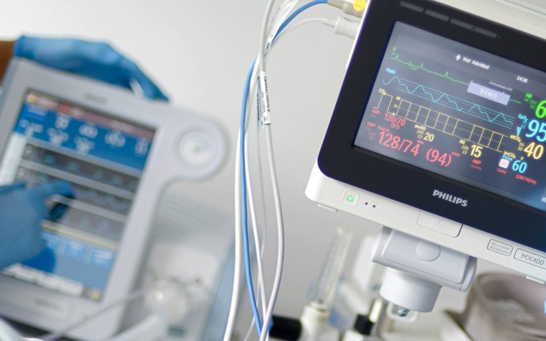
Electronic medical devices (EMDs) – also called “Healthcare Electronics” – play a vital role in today’s worldwide medical and healthcare settings, including medical offices, clinics, hospitals, long-term care facilities and home healthcare. EMDs have components for controlling the flow of electrical currents for the purpose of information processing and system control, including transistors, diodes and semiconductors. EMDs broadly include monitors, instruments, measurement and diagnostic equipment, point of care, therapy and testing devices, and other equipment. These device have electronic assemblies, semiconductors, integrated circuits which require thin and thick film for circuit design, adhesion and manufacturing purposes.
Microfluidics
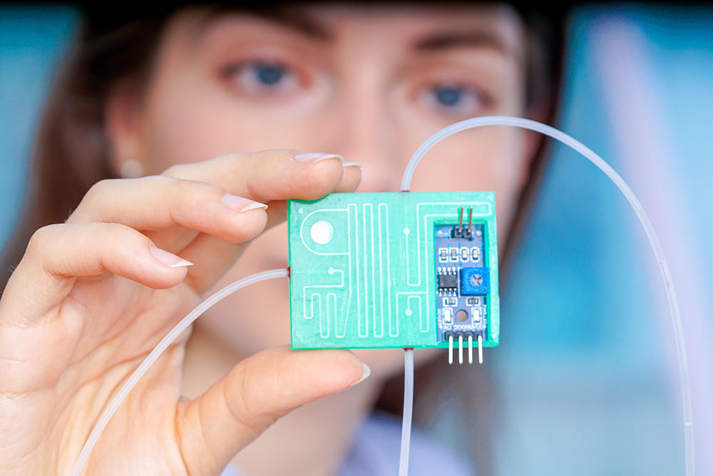
Microfluidic devices and systems enable the processing and detection of cancer and pathogenic particles for diagnostic and therapeutic purposes. Microfluidic products measure, manipulate and control fluids at microliter to picoliter levels in networks of channels with dimensions from tens to hundreds of microns. The manufacturing of these devices and systems require the manufacture in micro-miniaturized chambers and tunnels through which fluids flow or are confined. These life-saving devices are enabled by both thin and especially, thick film structures.
To learn more about thin thick film applications, email us at info@djmicrolaminates.com.


Stay Connected